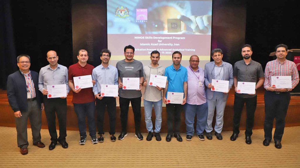
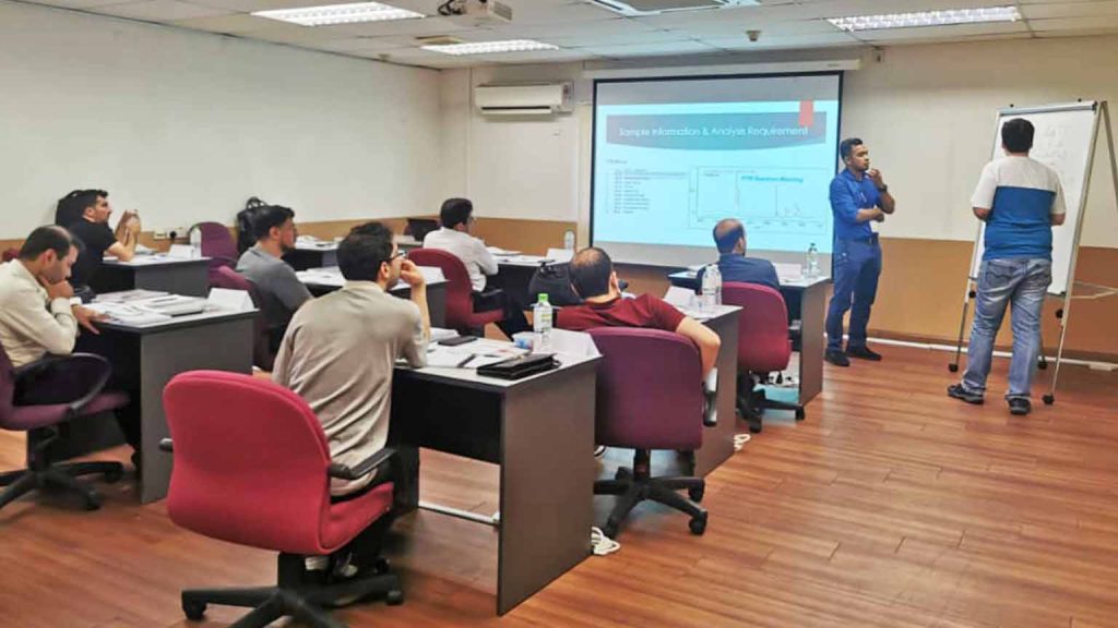
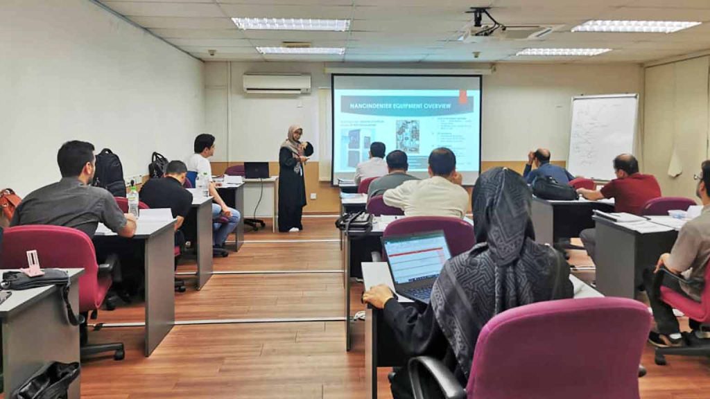
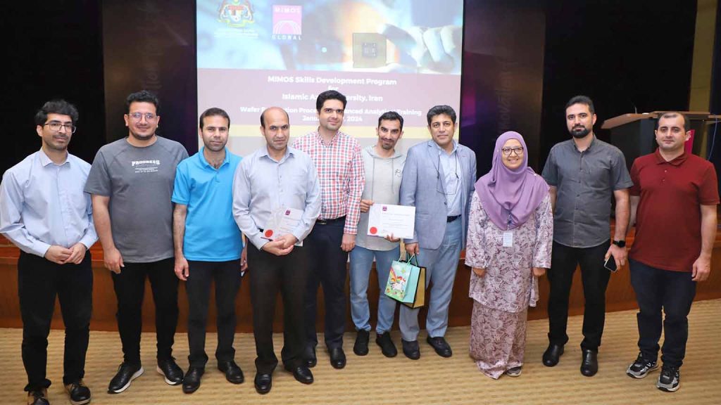
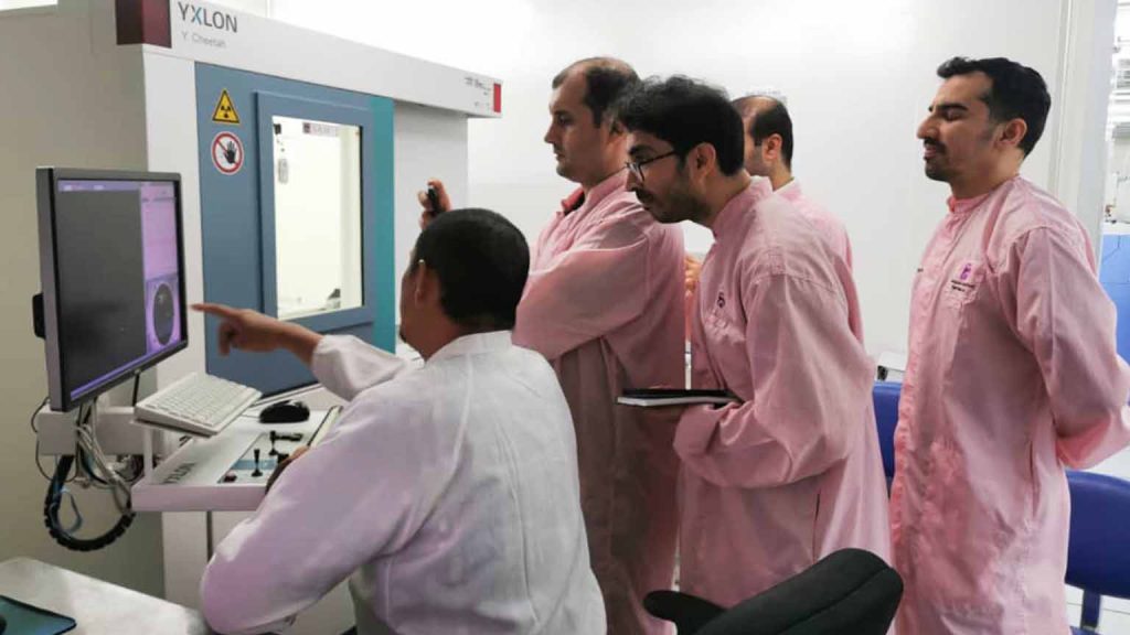
In a pioneering effort to bridge knowledge gaps and enhance the expertise of international scholars in semiconductor technologies, the MIMOS Semiconductor Technology Centre (STC) Team started the year by conducting a comprehensive week-long training session on the Wafer Fabrication Process & Advanced Analytical Training from 8 January to 17 January 2024.
This meticulously curated programme welcomed nine participants, including a distinguished professor, Clean Room Specialists, and PhD students from the Islamic Azad University, Iran. This diverse group embarked on a deep dive into the intricate world of semiconductor fabrication, with a keen focus on the theoretical and practical aspects of CMOS Integrated Circuit and MEMS development.
The training was designed with a dual objective, retraining and upskilling the participants for advanced courses, and providing them with a robust overview of wafer fabrication alongside exposure to crucial characterisation services.
The sessions, rich in content and hands-on experiences, covered a wide array of topics aimed at equipping the attendees with the latest techniques and knowledge in the field. Participants were introduced to the complexities of material analysis, the intricacies of failure analysis, and the comprehensive nature of reliability testing services.
This unique opportunity not only allowed them to gain valuable insights into the application of these analyses but also fostered an environment of learning and collaboration among industry experts and academics. By the end of the training, the Azad University team was poised to bring back advanced skills and a deeper understanding of semiconductor technologies, marking a significant step forward in their academic and professional journeys.
The MIMOS STC’s commitment to advancing global knowledge exchange and technical proficiency was showcased through this initiative, setting a new benchmark for international collaboration and technical education.
