Overview
MIMOS Semiconductor Technology Centre provides several Industry-standard wafer fabrication technologies based on 200mm wafers at small volume capacity. The 200mm wafer fabrication plant (FAB) is fully equipped with industry-standard technology as well as machinery, to meet a variety industrial and research needs.
The Centre also provides turnkey design support, customised processes, Multi-Project Wafer (MPW) programmes, as well as product development & fabrication in CMOS, Power MOSFET, Schottky rectifier diode, digital, analogue, and Micro/Nano Electro Mechanical Systems (MEMS/NEMS) technology platform.
Wafer fabrication technologies based on 200mm wafers at small volume capacity. The 200mm wafer fabrication plant (FAB) is fully equipped with industry-standard technology.
Technology Summary
| Technology Platform | Process Technology | Process Description |
Features |
| CMOS | 0.35μm |
CMOS Analog/Mixed Signal Technology |
2P3M, 3.3V I/O, Device Model Verification |
| 0.5μm |
CMOS Analog/Mixed Signal Technology |
2P2M, 5.0V I/O, Device Model Verification | |
| Power MOSFET | 0.2μm | Trench HVNMOS |
Low RDSon, Trench, 20V and 30V Manufacturing Proven |
| 0.4μm | Trench HVNMOS |
Low RDSon, Trench, 60V and 70V Manufacturing Proven |
|
| Schottky Diode | 0.4μm | Trench Schottky Diode | Low Vf, 45V and 60V Manufacturing Proven |
|
Carbon Nanotubes |
PECVD |
Carbon Nanotubes on Wafer |
Multi-wall CNTs, aligned |
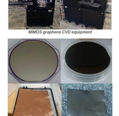
| Graphene | CVD | Graphene on Catalyst Wafer | Single Layer/Multi-layer Graphene |
| Nanowires/ Nanoparticles | PECVD | Nanowires/Nanopar ticles on Wafer – |
Nanowires: Silicon, Zinc Oxide Nanoparticles: Ferromagnetic (Co, Ni, Fe), Metallic (Pt, Au) and others |
| Zinc Oxide Nanowires | Hydrothermal |
Low Temperature ZnO Nanowires on Wafer |
Temperature: <100°C |
-
CMOS Technology
Complimentary Metal-Oxide-Semiconductor (CMOS) is one of the most popular technology used in logic integrated circuit design in numerous electronic applications. It has several key advantages with smaller power dissipation that suitable for computing, communication, and consumer electronics. This technology uses both NMOS and PMOS transistors for logic circuit design. There are two process technology nodes (0.5 μm and 0.35 μm) available in MIMOS Wafer FAB and it comes with a complete process design kit (PDK).
-
Power MOSFET Technology
Power MOSFET technology is used for high power applications such as power supplies, DC-to-DC converters, automotive electronics, motor controllers, etc. The technology is based on metal-oxide-silicon field-effect transistor vertically designed to operate at high level of power with high switching speed and good efficiency. The operating principle of power MOSFET is also similar to the normal MOS transistors except for high power handling capability. It has a compact transistor design with the smallest geometry of 0.2 μm.
-
Schottky Diode Technology
Schottky diode technology is used for rectifying a current from conducting state to blocking state. The main advantages of Schottky diode include low forward voltage drop, fast switching speed approaching zero-time and low-loss at high operating frequency, which ideal for many applications such as RF mixer & detector, power rectifier, switching power supply, solar cell, clamp diode, etc. Trench MOS barrier Schottky (TMBS) diode design concept is used in MIMOS Schottky diode technology to minimise the leakage current and maximise the current density of the diode with blocking capability up to 60V
-
Nanofabrication Technology
MIMOS Nanofabrication Technology includes specialised process technologies developed in-house through a novel process integration of traditional top-down wafer fabrication processes with leading edge bottom-up nanomaterials synthesis on a full-scale 200mm wafer or on a selective region.
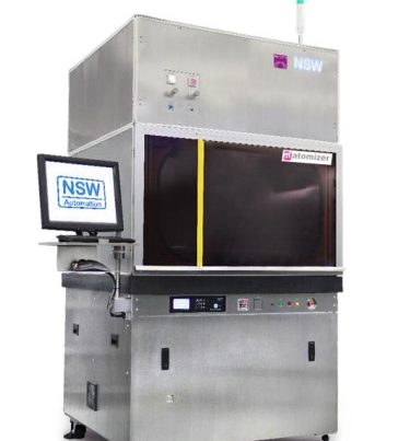
This technology utilises our state-of-the-art facilities in MIMOS wafer FAB for high-specification nanofabrication and nanomaterials synthesis. Among the nanofabrication and nanomaterials developed in the FAB include nanomaterials ultrasonic spray coating, CVD graphene, hexagonal Boron Nitride (hBN), Carbon Nanotubes (CNTs), Nanowires, Nanoparticles and their hybrid derivatives. The following are some of the nanofabrication technologies developed in the MIMOS Wafer FAB.


